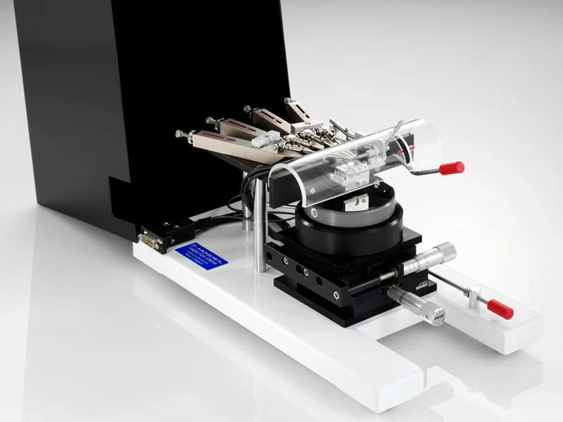
Semiconductor Equipment, Spare Parts & Services in Europe

MDC Europe is your trusted partner for semiconductor spare parts, refurbished equipment, calibration, and technical services. From wafer process to backend, we provide reliable and cost-effective solutions to support your production lines and research facilities.

MDC Europe office
MDC Europe office mobile mini

Our Products

Explore our comprehensive range of semiconductor spares and equipment, designed to ensure reliability, precision, and long-term performance.

Optics, mechanics, probe heads, gold parts, chucks, and more – refurbished to OEM-level quality.

Optics, mechanics, probe heads, gold parts, chucks, and more – refurbished to OEM-level quality.

Optics, mechanics, probe heads, gold parts, chucks, and more – refurbished to OEM-level quality.

Optics, mechanics, probe heads, gold parts, chucks, and more – refurbished to OEM-level quality.

Our Services

From calibration to refurbishment, MDC Europe offers tailored services to keep your tools running at peak performance.

Ensure accuracy and compliance with industry standards.

Prevent downtime and guarantee smooth operations.

Extend lifetime and upgrade your existing equipment.

Extend lifetime and upgrade your existing equipment.

four point probe station
Trusted by leading industry players for three decades

About MDC Europe

Founded in Switzerland, MDC Europe has more than 30 years of experience in semiconductor manufacturing solutions. We are proud to support OEMs, research institutes, and production fabs across Europe.

Our Clients & References

We are trusted by leading semiconductor manufacturers, OEMs, and research centers across Europe, including Bosch, ABB, CEA-Leti, GE and more.

FAQ

What are 'ohms per square'?

The unit of measurement when measuring the resistance of a thin film of a material using the four point probe technique. It is equal to the resistance between two electrodes on opposite sides of a theoretical square. The size of the square is unimportant and so strictly the measurement is in ohms, however ohms/square distinguishes measurement of a thin sheet from measurement of, for instance, a wire.

The unit of measurement when measuring the bulk or volume resistivity of thick or homogeneous materials such as bare silicon wafers or silicon ingots, using the four point probe technique.

The term Ohms.cm (Ohms centimeter) refers to the measurement of the “bulk” or “volume” resistivity of a semi-conductive material. Ohms.cm is used for measuring the conductivity of a three dimensional material such as a silicon ingot or a thick layer of a material. The term “Ohms-per-square” is used when measuring sheet resistance, i.e., the resistance value of a thin layer of a semi-conductive material. The equations for calculating bulk resistivity are different from those used to calculate sheet resistance, however, if the sheet resistance is known, bulk resistivity can be calculated by multiplying the sheet resistance in Ohms-per-square by the thickness of the material in centimeters.

To perform rapid, non-destructive electrical characterization of non-metallized planar semiconductors: SiC, GaAs, 2DEG, GaN, InP, CdS, InSb, etc. To substitute alternative methods which take several hours and require detailed metallization — characterization of thin epitaxial layers grown on silicon, thin-film characterization screening tool to conduct rapid integrity tests on various substrate surfaces. Mercury Probes can be connected to C-V plotters, curve tracers, doping profilers, computerized semiconductor measurement systems, CSM-WIN. Resistance can be measured on thin films composed of any material that does not react with mercury. Metals, semiconductors, oxides, and chemical coatings may be measured successfully. Mercury Probes can measure oxidized Silicon wafers or bare Silicon wafers. For MOS devices a darkbox is available to prevent light interference.

MOS production C-V measurements with or w/o bias-temperature stress with correction of series resistance effects. MOS ENGINEERING TESTS: MOS C-V and Conductance-Voltage plotting, theoretical MOS C-V curve generation and Dit computation, Capacitance-Time measurements (Zerbst analysis), doping profiling of sub-oxide regions, thin oxide analysis using the Ricco method, quantum effects and polysilicon depletion. JUNCTION TESTS: adaptive C-V data gathering for doping and resistivity profiles, junction series resistance and built-in potential. VARIABLE FREQUENCY MOS C-V TESTS. MULTIPLE FREQUENCY C-V TESTS. QUASI-STATIC / Dit TEST. GOI TESTS (hardware dependent): gate oxide integrity using forced, ramped, or pulsed voltage and current sources, histograms, TDDB plots, Weibull plots. I-V TESTS: current voltage characteristics of junction and MIS structures and oxide breakdown tests. THIN OXIDE PROGRAMS: Frequency-Shifting data gathering. CVC Analysis functions for quantum effects and polysilicon depletion effects.

Why to Choose Us?

  • 30+ years of experience in semiconductor solutions
  • OEM-level refurbishment quality
  • Fast European delivery & support
  • Comprehensive portfolio from spares to services
  • Partnership with leading OEMs
MDC-Europe_background

Contact our experts

Need a quote, a spare part, or technical support? Our team is here to help you within 24 hours.